CD4051BE
Texas Instruments · Logic ICs · PDIP-16, 7.62 mm row pitch · Through-hole
Profile cd4051be Profiled: 16 Oct 2026
Lifecycle: Active
Availability risk: Low
Specification
Transcribed from the manufacturer datasheet
| Function | Single 8-channel analogue multiplexer/demultiplexer |
|---|---|
| Supply range | 3 V to 18 V (Vdd - Vss) |
| On resistance | 125 Ω typical at 15 V, 250 Ω at 5 V |
| On resistance match | ±5 Ω between channels at 15 V |
| Leakage | ±100 pA at 25 °C, off channels |
| Bandwidth | ~20 MHz at 15 V, 7 MHz at 5 V |
| Tolerance | Rds(on) matched to ±5 Ω between channels at 15 V |
| Voltage rating | 3 V to 18 V total supply; analogue signal must stay within Vss to Vdd |
| Lifecycle | Active |
| Datasheet reference | Texas Instruments CD4051B datasheet, doc SCHS047, rev. 2023-03, §6.5 (on-resistance vs supply) and the truth table in §8.2 |
|---|---|
| Manufacturer | Texas Instruments |
| Mounting | Through-hole |
Substitute graph
3 Alternates
Interchangeable part numbers for this profile. A solid node is already profiled in this catalogue; a hollow node is a valid substitute that has no profile yet.
-
CD4051BM not yet profiled
SOIC-16 version of the same die. Same function, smaller and cheaper; the correct choice for new surface-mount designs and not compatible with a DIP socket.
-
CD74HC4051E not yet profiled
HC family version with 70 Ω on-resistance at 5 V, roughly a third of the CD4051 at the same supply. Far better for low-voltage designs; the lower resistance also means a higher leakage and a smaller maximum supply of 6 V.
-
ADG708BRUZ not yet profiled
Analog Devices 8-channel mux with 4.5 Ω on-resistance, 2.5 pA leakage and rail-to-rail operation. Roughly 15x the price and worth every cent when the source impedance is above a few kilohms, because 125 Ω of switch resistance ruins the accuracy of a high-impedance measurement.
Selection notes
The only prose on this page
125 Ω is the number that decides if you can use it
The switch resistance adds directly to the source impedance. Feeding a 12-bit ADC with a 10 kΩ source through a 125 Ω switch is fine, because the switch adds 1.2 % of error that a calibration removes. Feeding a 1 MΩ source through it is not: the switch forms a divider with the ADC's input impedance and the reading collapses. Keep source impedance below about 10 kΩ, or buffer each channel.
On-resistance varies with signal level
The switch is a CMOS transmission gate, and its resistance changes as the signal moves away from the rails — typically rising 30-50 % from mid-supply to near Vdd. That variation is why a multiplexed signal shows a small level-dependent gain error per channel. At 15 V supply and ±5 Ω channel matching, the variation between channels is small; at 5 V the matching is worse and the effect is larger.
Break-before-make and charge injection
The 4051 breaks the old channel before making the new one, so there is a brief open circuit during the transition — that is generally what you want, but with a high-impedance load the output floats during the interval. Charge injection of a few picocoulombs also puts a small step on the output at each switch, which a slow ADC will integrate into the reading. Allow 1-2 µs of settling after a channel change.
Sources
Texas Instruments — https://www.ti.com/lit/an/slva840/slva840.pdf · AEC — https://aecouncil.com/Documents/AEC_Q100_Rev_H_Base_Document.pdf · NIST — https://www.nist.gov/standardsgov/compliance-faqs-rohs
| Sourcing — Availability risk | The 4051 is a long-lived commodity in the CD4000 logic family. TI, Nexperia, onsemi and several Asian manufacturers produce it, in DIP and surface-mount, with no meaningful shortage history at any point in the last three decades. |
|---|---|
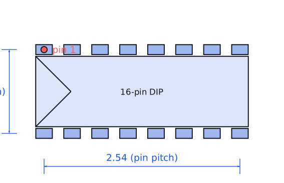
| Pinout and handling | PDIP-16. Pins 9, 10 and 11 are the binary channel select inputs A, B and C; pin 6 is the inhibit (active high, tie low to enable); pins 13, 14, 15, 12, 1, 5, 2 and 4 are channels Y0 to Y7; pin 3 is the common Z. The analogue signal must not exceed Vdd or go below Vss — there is no clamping, and exceeding the rails forward-biases the internal protection diodes into the substrate. |
Engineering information only. Verify every substitution against the manufacturer datasheet and your own operating conditions before committing a design. No pricing or vendor links appear on this page.