BZX84C5V1
Multiple (Nexperia, Vishay, onsemi, Diodes Inc) · Diodes · SOT-23 (3-lead, 2 used) · SMD
Profile bzx84c5v1 Profiled: 09 Sep 2026
Lifecycle: Active
Availability risk: Low
Specification
Transcribed from the manufacturer datasheet
| Type | Zener diode, 5.1 V nominal |
|---|---|
| Zener voltage | 4.8 V to 5.4 V at 5 mA (C suffix = ±5 %) |
| Power dissipation | 300 mW at 25 °C ambient, derate 2.4 mW/°C |
| Impedance | 60 Ω max at 5 mA, 480 Ω max at 1 mA |
| Temp. coefficient | -1.4 mV/°C near 5 mA |
| Reverse leakage | 1 µA max at 2 V |
| Tolerance | ±5 % (C suffix) |
| Voltage rating | 5.1 V zener, 300 mW |
| Lifecycle | Active |
| Datasheet reference | Nexperia BZX84 series datasheet, rev. 2023-11, Table 7 (Vz and impedance bins) and Fig. 5 (temperature coefficient vs Zz) |
|---|---|
| Manufacturer | Multiple (Nexperia, Vishay, onsemi, Diodes Inc) |
| Mounting | SMD |
Substitute graph
3 Alternates
Interchangeable part numbers for this profile. A solid node is already profiled in this catalogue; a hollow node is a valid substitute that has no profile yet.
-
BZX84B5V1 not yet profiled
±2 % tolerance version of the same die. Costs about 20 % more and is the honest choice when the zener actually sets a reference rather than protecting a gate.
-
MMBZ5231BLT1G not yet profiled
onsemi 5.1 V 225 mW zener in the same SOT-23 outline. Slightly lower power rating; otherwise interchangeable. Watch the power derating if the diode is a clamp rather than a reference.
-
TLZ5V1B not yet profiled
Vishay 5.1 V zener with a tighter impedance spec and lower knee current. Better regulation at 1 mA, roughly 2x the price. Use it if the zener has to hold a rail at microamp bias.
Selection notes
The only prose on this page
Why 5.1 V beats 5.6 V for a reference
Zener temperature coefficient crosses zero near 5.6 V for a classic zener and near 5.1 V is still negative at about -1.4 mV/°C. That -1.4 mV/°C is -0.027 %/°C, which over a 60 °C swing is a 1.6 % drift — fine for gate protection, poor as a voltage reference. If you need a real reference, use a bandgap device; a zener is a clamp that happens to have a known voltage.
Impedance sets the usable bias range
The 60 Ω impedance at 5 mA becomes 480 Ω at 1 mA. That means the same zener holds its voltage eight times worse at low current, so a zener biased through a 100 kΩ resistor from 12 V is a very poor regulator. Practical rule: bias a BZX84 with at least 2-5 mA if you care about the voltage at all, and accept 30-100 mW of standing dissipation.
Clamping role and the 300 mW limit
As a gate clamp on a MOSFET, the zener must absorb the energy stored in the gate circuit during turn-off. At 300 mW continuous and a 2.4 mW/°C derating, a board at 70 °C has only 192 mW available. A 12 V gate drive through a 10 Ω resistor into a 5.1 V zener is fine (about 0.5 W for nanoseconds), but a sustained overvoltage is not. If the zener has to survive continuous clamp duty, size it for the actual power, not the pulse.
Sources
Vishay Semiconductors — https://www.vishay.com/docs/81857/1n4148.pdf · Texas Instruments — https://www.ti.com/lit/an/slva840/slva840.pdf · NIST — https://www.nist.gov/standardsgov/compliance-faqs-rohs
| Sourcing — Availability risk | Zeners are a commodity in every SOT-23 catalogue; 5.1 V is one of the two or three most common values because it is the closest standard zener to a 5 V rail. No allocation history and no single-source exposure. |
|---|---|
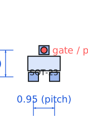
| Pinout and handling | Polarised: the cathode is the banded end in the schematic, and in SOT-23 the two used pins are 1 (anode) and 3 (cathode) for most manufacturers, with pin 2 unused or internally connected to the cathode on some versions. Always confirm pin 2 on the specific datasheet — it is not consistent across the second sources. |
Engineering information only. Verify every substitution against the manufacturer datasheet and your own operating conditions before committing a design. No pricing or vendor links appear on this page.